LPDDR5 Upgrades: Boosting IoT, AI & Image Processing

VIP Expert

Feb 21, 2018 / 3 min read

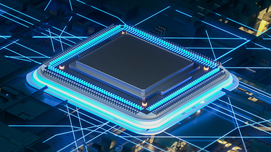
New applications like Cloud Computing, Artificial Intelligence, Autonomous cars, Augmented reality, Embedded vision are driving stricter requirements around memory performance and power efficiency.  Memory is central to these systems, that require high bandwidth and speed along with lower power and lower cost. With these emerging market needs, the memory industry started to move from planar (2D) DRAMs to wide I/O or a 3D technology TSVs (Through Silicon Vertical interconnect access) such as HBM (high bandwidth memory). For more insight on HBM, read our blog “Next Generation Memory Technology for Graphics, Networking and HPC.”  Low Power DRAM technology, evolved to the fifth-generation(LPDDR5) to deliver significant reduction in power and extremely high bandwidth as compared to LPDDR4. In this blog, we discuss LPDDR5 new features based on our understanding from collaboration with memory vendors and early adopters of Synopsys VIP over last 2 years.

LPDDR5 evolution chart

LPDDR5 increases the data bandwidth while maintaining options to save power using the deep sleep mechanism. Some of the key features of LPDDR5 are as per following: –

  • Bandwidth: Memory bandwidth is very important across the emerging applications, for example high speed gaming requiring low latency, or transmission of big data like in 1080p, 4K videos, or slow-motion videos. LPDDR5 can support bandwidth upto 6400 Mb/s.
  • Link ECC: LPDDR5 will support Link ECC functionality for Read and Write Operation to recover the data even when errors are introduced either due to transmission or due to storage (charge loss) of data. DMI (Data Mask Inversion) signal will be used as parity signal during read operation and RDQS (Read Data Strobe) signal will be used as parity signal during write operation.
  • DSM: Deep Sleep Mode (DSM) is used to reduce IDD current by 40%. DSM can be issued in idle state or in self refresh state. DSM state time is relatively longer (approx. 4ms) because DSM includes Deep Power Down and Self Refresh. In DSM, all input buffers, all output buffers, and the power supply to internal circuitry may be disabled within the DRAM.
  • Data Copy: Data copy is a low power function to reduce LPDDR5 IO and core power (IDD4W, IDD4R) consumption by utilizing data pattern repeatability per 8Byte data copy granularity. The LPDDR5 Data Copy Low Power function is added on normal Write, Mask Write, and/or Read operations with the same latencies and AC timing conditions.
LPDDR5 clock ratio diagram

  • WCK Clock: LPDDR5 introduces WCK clock, similar to GDDR5. LPDDR5 operates at two differential clocks CK_t and CK_c, while data interface uses two differential forward clocks WCK_t and WCK_c. WCK_t and WCK_c can operate at two times or four times the frequency of command/address (operation) clock (CK_t/CK_c). In the example below WCK_t and WCK_c is used to sample DQ data for write operation and toggle DQ (data) for read operation.
LPDDR5 clock table

Synopsys is engaged with the early adopters of LPDDR5 Verification IP, which has been available since 2016. For more information on Synopsys memory VIP, please visit http://synopsys.com/vip. Stay tuned for upcoming blogs on LPDDR5. Our recent blogs on next generation DRAM and Flash memory technologies: –

Continue Reading