Synopsys Cloud
Cloud native EDA tools & pre-optimized hardware platforms
Request a Free Trial →
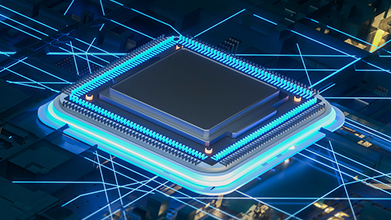
The DDR PHY Interface (DFI) is used in several consumer electronics devices including smart phones. DFI is an interface protocol that defines signals, timing, and programmable parameters required to transfer control information and data to and from the DRAM devices, and between MC (Micro Controller) and PHY. DFI is applicable to all DRAM protocols including DDR4, DDR3, DDR2, DDR, LPDDR4, LPDDR3, LPDDR2 and LPDDR.
The DFI interface is not necessary when the MC and PHY are being developed specifically to work together. However, in many situations, the MC and PHY are designed separately – often by different companies. DFI permits companies to develop both MC and PHY IP designs knowing that they will be able to interoperate with the devices developed by other companies.
Additionally, MC devices are primarily clock-based, whereas PHY generally consists of a significant amount of analog logic, therefore the two devices are often developed by different engineers even within the same company. DFI creates a well-defined interface for the two separate design teams.

DFI in Memory System
The latest DFI spec version is 4.0, revision 2. The spec has undergone several major enhancements over the years as shown in following table: